Ⅰ. 골밀도측정기
골다공증을 정확하게 진단하려면 골생검이 필요하지만 환자에게 고통을 준다는 점에서 쉽게 시행할 수 없는 검사로 알려져 있다. 따라서 최근에는 골다공증을 진단하는데 골밀도 측정기에 의한 방법이 흔히 이용되고 있다. 골밀도가 골다공증의 진료에 이용될 수 있는 이유는 골밀
가. 기존 폴리머 태양전지의 한계
1) Active Layer를 구성하는 물질들의 Mobility가 낮기 때문에 100nm 이상의 두께를 초과하면 효율이 감소한다. 허나 대부분의 빛을 흡수하려면 300nm정도의 두께가 필요하기 때문에(이것도 실리콘 태양전지-마이크로 단위-보다 훨씬 얇은 두께이다.) 수광률이 떨어진다.
2) E
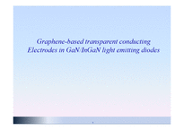
We investigated graphene-based transparent electrodes for InGaN/GaN light emitting diodes(LED). Nano-dotted layer of Ag and Ni were inserted between p-GaN and graphene to achieve low contact resistance and high transmittance. Heat treated Ag layer/graphene had low contact resistance of 0.7~1.2Ω/cm2, and we could achieve better luminance for GaN-based LED. However, for patterned Ni layer/graphene
2. Transparent Electrodes
투명 전극 (transparent electrodes)
가시광 영역의 빛을 투과 & 전기 전도성을 가지는 기능성 박막전극
유연성을 가짐
평판디스플레이, 터치패널, 태양전지 등의 전극기판으로 널리 이용
→ 정보전자 에너지 분야의 핵심 부품 소재
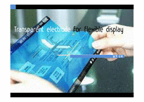
flexible display용 투
that subject.
Organic Solar cell
태양에너지를 전기에너지로 변환시키는 유기태양전지의 원리 및 특성 이해.
유기태양전지의 효율성 향상 방안 탐색
Direction of Idea
Replacing the electrode by using multi-layer matirials.
Using the non-perfectly used solar ray by the microcavity effect.
Using the conductive polymer to transparent electrode.
organic light emitting diode(OLED)
LED's emissive electroluminescent layer is composed of a film of organic compounds.
This layer of organic semi-conductor material is formed between two electrodes, where at least one of the electrodes is transparent.
OLED can be used in many display devices.
Active matrix OLED has an integrated electronic backplane made from thin film transistor
metal substrate를 지지대로 붙어 있기 때문에 p-type electrode가 n-type보다 아래쪽으로 오도록 배열시킨 특이한 구조이다. 또한 아랫부분에 Sapphire substrate를 제거시킨 것이 특징이다.
Metal substrate가 p-electrode의 역할을 하기 때문에 transparent conduction layer가 없이도 normal led에 비해 넓은 반응 면적을 가질 수 있다.
electrodes, respectively.
An exciton is a bound state of an electron and hole which are attracted to each other by the electrostatic Coulombic force.
The exciton diffuses to around by chemical potential.
The lifetime <<1 nano seconds
The average distance <<10 nanometer.
The exciton diffuses to the interface between two layers
The exciton is saparated by an electron an
efficiency
-Difficult to scale for large screen sizes
conclusion
OLED stands for Organic Light Emitting Diode
Low power consumption, ultra slim, formation of exciton by electron and hole recombination → rapid speed of response , wide viewing angle above 170°
- Characteristic of AM(Active Matrix) OLED
: transparent, flexibility in design, ecofriendly (lamp)
- Facing subject
Transparency & flexibility
Embodiment various colors
Low development cost
Environmental Friendliness
An infinitude of applications
- Portable charger, Clothing/Leisure industry, etc.
- Building Integrated PV(BIPV)